Welcome to the dedicated TINA Video Tutorials page, a valuable resource of educational content aimed at helping you master the intricacies of TINA software. In today’s fast-paced technological landscape, the ability to design, analyze, and simulate electronic circuits efficiently is paramount, and TINA Design Suite stands as a powerful tool to meet these challenges. Here, we delve into the world of TINA Video Tutorials, designed to cater to individuals at all levels of expertise.
For those just starting their journey into circuit simulation, these Video Tutorials provide a solid foundation. Beginners can explore fundamental aspects of the simulation environment, gaining insights into creating and analyzing electronic circuits. These tutorials serve as a gentle introduction, gradually acquainting you with TINA’s user-friendly interface and its wide array of features.
Other TINA Video tutorials delve deeper into the intricacies of TINA, such as comparing simulations to real-world measurements. By studying AC analysis and Fourier analysis, you’ll be equipped with the skills to analyze circuit behavior under different conditions. You’ll also learn how to create subcircuits from schematics, enabling modular circuit design and reuse.
For advanced users, TINA Video Tutorials offer a deep dive into the software’s advanced capabilities. You can explore topics like interactive logic gate testing, VHDL circuit design, and PCB development. These advanced features empower you to tackle complex circuit design challenges with confidence, precision, and efficiency.
These selected video tutorials provide step-by-step guidance, ensuring that you not only understand the concepts but also gain practical experience. The goal is to equip you with the tools and insights needed to unlock TINA’s full potential, enabling you to design and analyze circuits with precision and ease.
8051 Microcontroller Course- Embedded C and Assembly Language
Topic
Video
Introduction to TINA Design Suite
Comparison of simulation and real time measurements
Real time transient recording and comparison with simulation
RC transient and AC analysys
Fourier analysis
Active band pass filter
How to make subcircuits from schematics
Test a logic gate in interactive mode
Bus example
Pic flasher circuit
VHDL circuits
Create a simple PCB
Importing SPICE Models into TINA
The Art of Doing: Electronics for Everyone
Start designing, building, and playing with your own circuits today!!
In this article, we will explore the ESD Generator SPICE Simulation using an LTSpice model, shedding light on how this powerful tool can help analyze and enhance ESD protection strategies in electronic circuits.
ESD generator, also known as an “Electrostatic Discharge Generator,” is a device used in industrial and testing environments to simulate controlled and repeatable electrostatic discharges (ESD), which are sudden and brief electric currents that can damage or disrupt other electronic equipment. These generators are employed to test the resistance of electronic devices and circuits to simulated electrostatic discharges, assessing how these devices react and whether they are adequately protected against ESD-induced damage.
ESD generators can simulate different types of ESD pulses, such as those defined by various standards and applications. For example, some ESD generators can produce pulses that mimic the human body model (HBM), the machine model (MM), or the charged device model (CDM) of ESD. Some ESD generators can also produce pulses that comply with the requirements of the International Electrotechnical Commission (IEC) 61000-4-2 standard, which specifies the test levels and methods for evaluating the ESD immunity of electrical and electronic equipment.
To take your first steps with LTSpice simulation software, you can read this article.
Università Politecnica delle Marche, Ancona, Italy.
by
Ing. Luca Buccolini
A SIMPLE SPICE ESD GENERATOR CIRCUIT BASED ON IEC61000-4-2 STANDARD
WHAT IS ESD?
Static charge is an unbalanced electrical charge at rest. Typically, it is created by insulator surfaces rubbing together or pulling apart. One surface gains electrons, while the other surface loses electrons. This results in an unbalanced electrical condition known as static charge.
When a static charge moves from one surface to another, it becomes ESD. ESD is a miniature lightning bolt of charge that moves between two surfaces that have different potentials. It can occur only when the voltage differential between the two surfaces is sufficiently high to break down the dielectric strength of the medium separating the two surfaces.
When a static charge moves, it becomes a current that damages or destroys gate oxide, metallization, and junctions. ESD can occur in any one of four different ways: a charged body can touch an IC, a charged IC can touch a grounded surface, a charged machine can touch an IC, or an electrostatic field can induce a voltage across a dielectric sufficient to break it down
ESD STRESS MODELS
ESD can have serious detrimental effects on all semiconductor ICs and the system that contains them. Standards are developed to enhance the quality and reliability of ICs by ensuring all devices employed have undergone proper ESD design and testing, thereby, minimizing the detrimental effects of ESD. Three major stress methods are widely used in the industry today to describe uniform methods for establishing ESD withstand thresholds (highest passing level).
HUMAN BODY MODEL (HBM)
The HBM is a component level stress developed to simulate the action of a human body discharging accumulated static charge through a device to ground, and employs a series RC network consisting of a 100 pF capacitor and a 1500 Ohm resistor.
CHARGED DEVICE MODEL (CDM)
The CDM is a component level stress that simulates charging and discharging events that occur in production equipment and processes. Potential for CDM ESD events occur when there is metal-to-metal contact in manufacturing.
SYSTEM LEVEL ESD (IEC 61000-4-2)
The IEC system level ESD is a widely accepted European standard that defines an ESD event that is meant to be tested on actual end equipment to simulate a charged person or object discharging into electronic systems. The IEC standard defines an ESD stress that is much stronger than the component level ESD stresses defined by HBM and CDM.
The engineer must design following IEC 61000-4-2 standard to be able to declare the conformity CE (“Conformité Européenne”).
The ESD generator circuit realized in this work is compliant with ESD generator used in EMC laboratories to perform CE-conformity tests, thus a SPICE simulation can be used to test ESD-immunity solutions before circuit production.
IEC 61000-4-2 WAVEFORM CHARACTERISTICS
The standard accurately describe the characteristics and performances of the ESD generator as well as the current waveform parameters.
The ESD phenomenon is a very short but very strong current transient and is represented in Figure 1.
Figure 1. 61000-4-2 ideal contact ESD waveform at 4kV
This pulse is divided into two parts: The first peak, known as the “Initial Peak”, is caused by the discharge of the arm, and generates the maximum current. The second peak is caused by the discharge of the body. The rise time of the initial peak is between 0.6 ns and 1 ns, and its amplitude depends on the charging voltage of the ESD simulator.
The standard describe a formula and the mains current level of the waveform for different test level.
Table 1 contact discharge current waveform parameters
Even though the IEC 61000-4-2 [2] include a simplified circuit of ESD generator, it is incompatible with the discharge current equation descripted in the standard and the waveform shown in Figure 1. A PSpice software simulation can prove this.
THE BASIC ESD GENERATOR MODEL
In order to run ESD stress simulation, an ESD-generator model was built. This can help engineers to test different solutions in a SPICE simulator to overcome strength over-voltages before realizing PCB circuit and test it against ESD.
The objective is to generate an ESD pulse that accurately corresponds to the current stress waveforms at various stress levels in accordance with the IEC 61000-4-2 specification.
The ESD can be simulated by two parallel R, L, C circuits with charged capacitors. The generator equivalent circuit is shown in Figure 2.
Here the standardized network elements of the ESD-generator are represented by R1 (330ohm) and C1 (150pF). The inductor L1 is considered to be the obligatory ground strap with the length of about 2 m. Physically the first peak of the pulse is shaped by additional lumped and parasitic elements around and in the tip of the ESD-generator [5].
Note that the values of R, L, and C for both branches are tweaked to correctly represent standard IEC stress waveform; “.ic V(c1)=4kV V(c2)=4kV” refers to the initial condition of the voltage on the capacitors for a 4kV zap.
Figure 2 The general equivalent circuit of basic IEC61000-4-2 generator model
Modeling in SPICE& a diode is not a trivial work. Although the operation of the diode is quite simple, extract a model from datasheet takes some time.Every component has its own syntax defined in SPICE , in the case of the diode:
.model ModelName D (par1=a par2=b………parn=x)
where par1 par2 …. parn are characteristic parameters of diode.
we can sum up the set of main parameters in the following table:
Parameter
Description
Unit
Default value
BV
Reverse breakdown knee voltage
V
Infinite
CJO
Zero-bias p-n capacitance
F
0
EG
Bandgap voltage
eV
1.11
FC
Forward-bias depletion capacitance coefficient
no unit dimension
0.5
IBLV
Low-level reverse breakdown knee corrent
A
0
IBV
Reverse breakdown knee corrent
A
1e-10
IKF
High-injection knee current
A
Infinite
IS
Saturation corrent
A
1e-14
ISR
Recombination current parameter
A
0
M
p-n grading coefficient
no unit dimension
0.5
N
Emission coefficient
no unit dimension
1.0
NR
Emission coefficient for ISR
no unit dimension
2.0
RS
Parasitic resistance
Ohm
0
TT
Transit time
sec
0
VJ
p-n potential
V
1.0
XTI
IS temperature exponent
no unit dimension
3.0
All these parameters are used by SPICE to describe the behavior of the diode in the different situations of signal, for example in direct polarization in DC that, forward current will be:
ID = IS*(e^(VD/(N*Vt))-1)
where VD is the forward voltage, Vt = k * T / q is the thermal voltage equal to 0.026 V at 27 degrees Celsius.
The so-called recombination current is instead calculated as
Irec = ISR*(e^(VD/(N*Vt))-1).
Other equations from the given parameters describing the capacitance of the junction, its evolution with temperature and more.
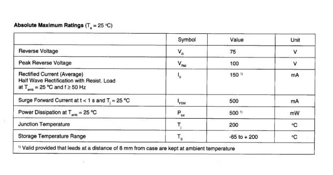
At this point we have to derive the various parameters from the datasheet of the component. Assume we want to model a silicon diode 1N4148. The extraction of the parameters of the table from the values reported in the datasheet, is not immediate for almost none of the parameters.look at the values of our interest in datasheet:
From the table we can get BV which is equal to VRM, in other cases reported as Vbr, or in the case of Zener diode Vz.
From this second table we see that the maximum leakage current at 25 degrees is Ir = 5 uA.We can take IBV as equal to 10 times Ir. Usually for this type of diodes the value of IBV is around 100uA. For Zener diodes Ir can be called Izk, or in other cases as Ibr.
CJO can be directly equal to the value specified in the datasheet as Cj or Ctot, in this case is 4pF.