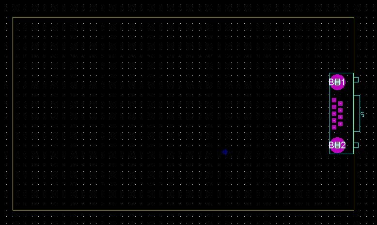
Let’s start the component placement process. We will utilize the automatic placement tool for all components, with the exception of connector J1, which we will position manually. Please select the component labeled J1 and manually place it on the side of the board, as illustrated in the following image:
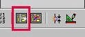
Proceed to position the remaining components. In this instance, we will employ the automatic placement tool for all the components. The tool’s icon is depicted as follows:
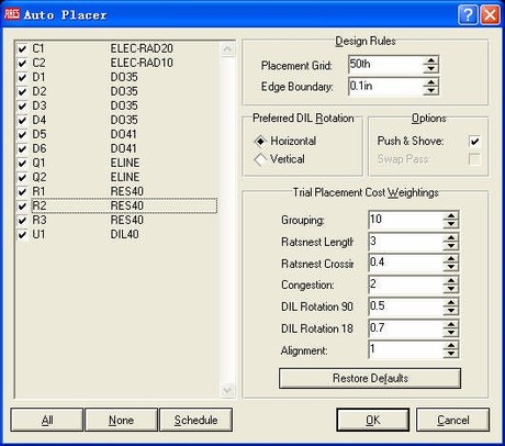
When the subsequent dialog box appears, leave the window settings unchanged and simply click ‘OK’ to proceed
As a result, the following configuration is achieved:
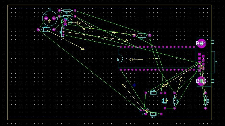
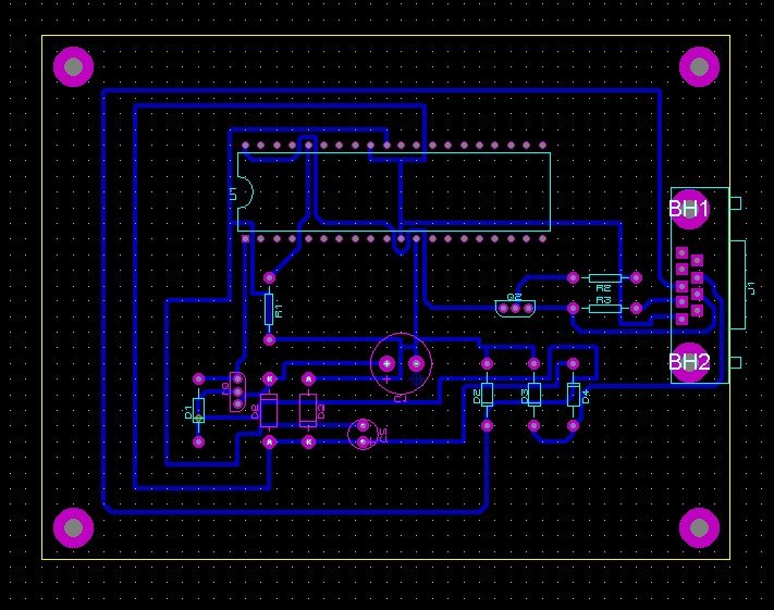
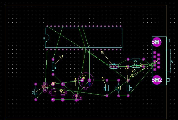
Now we neatly arrange the components and obtain:
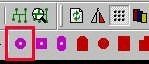
Here, we commence the process of connecting the components. Observe the icon in the image
Click on it to open the following dialog window
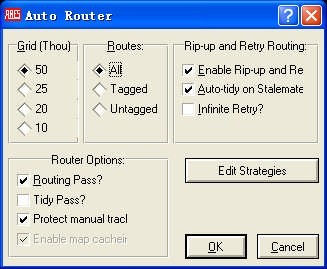
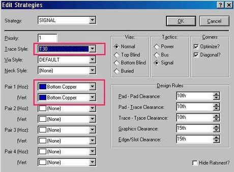
Click the ‘Set Strategies’ button to configure the routing strategy (rules). Open the dialog box as depicted in the figure below, and then select the ‘SIGNAL’ strategy with a single layer width of T30.
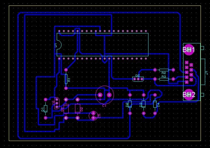
The automatic routing yields the following result:
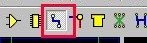
As the next step, we will make manual adjustments to the wiring and add four positioning holes. To initiate manual wire adjustments, you will need to click on the following icon, enabling modification of the wire:
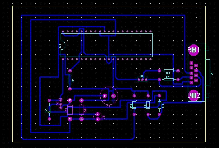
After making the necessary modifications, remember to switch to the desired layer for editing by selecting from the layer list located at the bottom of the main window. Here are the results after making these slight adjustments:
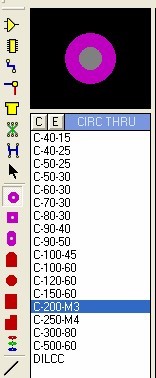
Now, let’s proceed to add four pads. Please click on the icon below to initiate this action
In the list, select the appropriate option for a circular pad.
This represents the final outcome: