Welcome to this LTspice tutorial! LTspice, developed by Linear Technology (now part of Analog Devices), is a robust and highly versatile SPICE-based electronic circuit simulation software that has become an invaluable tool for engineers, students, and hobbyists alike. In this tutorial, we will explore the remarkable features of LTspice that empower users to design, analyze, and refine electronic circuits with precision and efficiency.
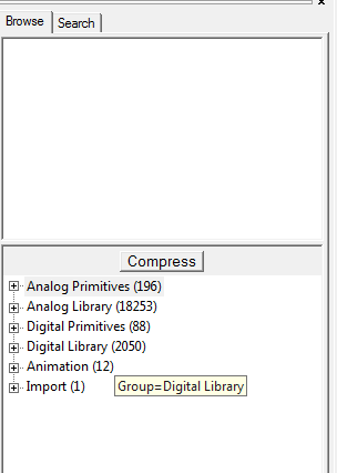
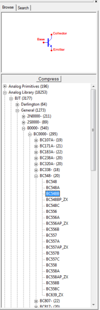
One of the standout features of LTspice is its extensive library of components. This library includes a comprehensive selection of analog and digital components, such as resistors, capacitors, inductors, transistors, op-amps, microcontrollers, and more. This expansive library ensures that users have access to a wide range of components to accurately model their circuits. Furthermore, we will show you how to add custom components to the library, enabling you to work with specialized or proprietary components specific to your projects.
Advanced simulation capabilities are another key strength of LTspice. It employs a powerful simulation engine capable of handling both transient and steady-state analyses. Through this tutorial, you will learn how to perform transient analysis to observe how a circuit responds over time, making it ideal for studying transient phenomena like start-up behavior and signal processing. You will also master steady-state analysis, allowing for the assessment of a circuit’s behavior under stable conditions, which is crucial for understanding its performance in practical applications.
LTspice’s ability to perform AC analysis is particularly useful for designing and analyzing circuits that operate with alternating currents. We will guide you through using this feature to evaluate the frequency response of a circuit, helping you optimize filter designs, amplifier performance, and more. Moreover, we will delve into Monte Carlo analysis and worst-case analysis tools, allowing you to assess the impact of component tolerances and variations on circuit performance—essential for designing robust circuits that can withstand real-world variations in component values.
The software’s user-friendly interface simplifies the process of schematic capture and modification. Throughout this tutorial, we will demonstrate how to easily draw circuit schematics and make changes with drag-and-drop functionality. The intuitive interface also allows for quick connections between components and nodes, reducing the time required to create complex circuit designs.
LTspice’s waveform analysis capabilities are indispensable for evaluating circuit behavior. You will learn how to plot waveforms, measure signal parameters, and perform Fourier analysis to examine frequency components in signals. This functionality is essential for troubleshooting and optimizing circuit designs.
One of the standout advantages of LTspice is its cost-effectiveness—it’s available for free! We will emphasize this throughout the tutorial, making it accessible to a wide audience, including students and hobbyists. Rest assured, this affordability does not compromise the quality or depth of its simulation capabilities, making it a top choice for educational institutions and professionals alike.
In conclusion, this LTspice tutorial aims to equip you with the knowledge and skills needed to harness the full potential of this remarkable software tool. Its extensive component library, advanced simulation capabilities, user-friendly interface, and affordability make it an indispensable resource for engineers and electronics enthusiasts. Whether you are a seasoned professional or a student learning the ropes of circuit design, LTspice provides the tools and capabilities needed to bring your electronic projects to life. So, let’s dive in and explore the world of LTspice together!
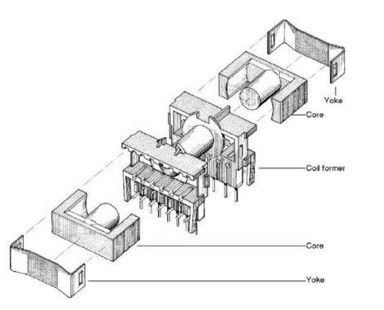
With this LTspice tutorial, we see how how to use LTspice for a Switching Mode Power Supply (SMPS) simulation:
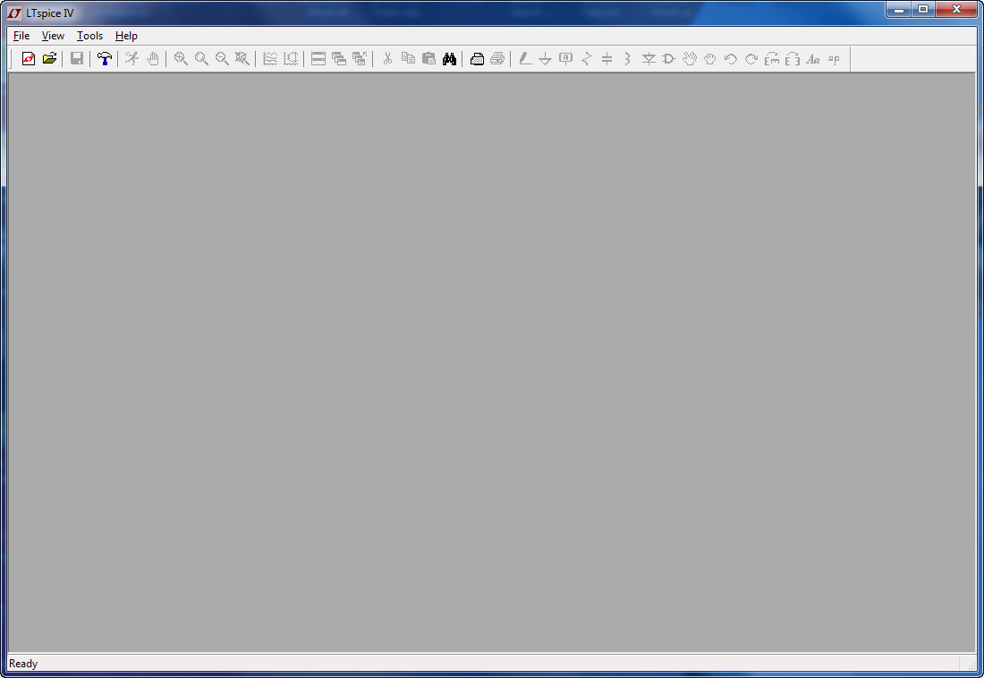
After installing LTspice, run the software:
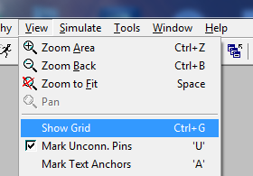
To initiate a new project, choose “New Schematic” and activate the grid

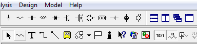
At the top toolbar, you can find the buttons to place all devices:
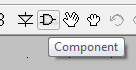
Select the Component Icon: