Help! – My board won’t route
Here are some suggestions for helping the autorouter.
1. If routing has almost worked (only one or two unrouted segments), try changing the hints given to the router. For the one-sided board there is only the suggested direction of tracks. It is best to unroute the board and begin afresh. Choose Edit > Delete Wires > All Wires from the menu bar of PCB Router or reload the unrouted version of your board in PCB Editor.
2. If you are far from success, look at the layout to see where the problems lie. Often one particular track prevents successful routing. Can you rearrange the components to solve the problem?
Quit from PCB Router without saving, or reload the previous version of your board in PCB Editor. Rearrange or reorientate components to make the ratsnest simpler and ease the problem before trying the autorouter again.
If none of this works, get advice from a more experienced PCB designer.

Figure 19. Cross-section of a double-sided printed circuit board showing free vias formed by a plated-through hole and a wire through a non-plated hole soldered top and bottom. A via can also be formed using a pin-through-hole component but not at a connector because it covers the top pad.
4.6 Final touches
Put your name on the bottom etch layer, run a final design rule check, save your routed board and make a coloured plot as before. My layout is shown in figure 18. It is a poor board in many respects despite the successful routing. The power tracks are excessively long in particular. It is not hard to see how the components could be rearranged to improve the layout.
5 Instrumentation amplifier – double-sided board
We will now route the board using both sides like many commercial PCBs. Having said that, use a single side wherever possible if your PCB is made using an old-fashioned process. Many problems occur with double-sided PCBs, mostly from badly placed vias, as I’ll now explain.
Figure 19 shows a cross-section of a double-sided PCB. Commercially produced PCBs have plated-through holes (PTHs), which means that the copper plating extends through the holes and joins the pads on the two sides of the board. A free via is a hole that is used purely to move a track from one side of the board to the other, rather than to mount a component. The plating carries current between the layers. Simple, manual processes cannot plate through holes, in which vias need more effort: A wire must be pushed through each hole and soldered top and bottom to join the layers of etch.
The wires of through-hole components can also be used as vias. This works well for some components, such as resistors and capacitors. However, it fails for others, such as connectors, because it is impossible to solder the pad on top of the board – it is hidden under the base of the connector. The pins of an integrated circuit can be used as vias if they are soldered directly to the board but it is safer to put ICs in sockets for PCBs that are assembled by hand and these hide the pads too. Vias must therefore be placed with great care if the PCB does not have plated-through holes.To illustrate these problems, figure 20 shows the two-sided layout of the instrumentation amplifier as it might come from the autorouter. (I should admit that I fiddled the layout to make it worse!) It obeys the design rules but is hard or impossible to assemble by hand.

Figure 20. Screenshot of a poor double-sided layout with several badly-placed vias.
• The board has five free vias, far too many for a board that could be routed successfully with only one layer. The worst via is under U3, which is unacceptable for a home-made via because the wire in the via would obstruct the integrated circuit. (There would be no problem on a commercial board with plated-through holes.) Another via is very close to the trimmer (R8) and it would be difficult to solder this without damaging the trimmer. You would have to solder the via first and keep it neat.
• Several pins of resistors act as vias – R3 has two, for instance. These are easy.
• The pins of the integrated circuits are connected to tracks on both the top and bottom.
This is not a problem if the IC is soldered directly to the board but won’t work if it is in a socket.
• The connectors (J1 and J2) and the trimmer (R8) have tracks only to the bottom of their pins. This is why the via is needed near R8. No tracks run to the top because the symbols for these components have route keepouts on the top, which forbid the router from placing tracks there. The footprints have diagonal shading in PCB Router to show this, visible in figure 16.
The general rule is to avoid vias wherever possible if your manufacturing process does not plate through holes. Every via requires two soldered joints (top and bottom), which dramatically reduces reliability.
Now route your board for the instrumentation amplifier using both sides.
1. Re-open the unrouted version of your board.
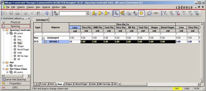
Figure 21. Constraint manager for changing the spacing around vias. The row of cells under Thru Via To has been selected and the value 25 typed into the first cell. This will fill the other cells selected after hitting the Enter key.
2. Remember the Default via padstack when you used the new board wizard? We specified VIA26. Unfortunately this has a bug because another type of via called simply VIA appears in the design and is used wrongly by default. This VIA is much too small so we must get rid of it.
Fixup. Choose Setup > Constraints > Physical. . . from the menu bar and select the upper All Layers spreadsheet under Physical Constraint Set. This resembles figure 13 but has only a DEFAULT row. The column headed Vias probably shows VIA:VIA26. Click in this cell to open the Edit Via List. Remove VIA from the Via list on the right and click OK. The cell now contains only VIA26, which is what we want.
Close the Constraint Manager and return to PCB Editor.
3. The new board wizard set up several spacings based on the minimum line width of
25 mils. Unfortunately it does not set up the spacing around vias, which is only 5 mils by default. This is too small for reliable construction by hand and should be increased to match the other spacings.
Fixup. Choose Setup > Constraints > Spacing. . . from the menu bar to open the Constraint Manager and select All Layers > Vias as in figure 21. Drag the mouse to select all the cells under Thru Via To in the DEFAULT row. Type 25 and hit Enter, which copies this value into all cells selected. Close the Constraint Manager and save your
board.
4. Run the autorouter from within PCB Editor or export the board to PCB Router as before.
This time you should allow routing on both layers, which is the default. You might like to experiment with the directions. Note the routed length and the number of vias; a good
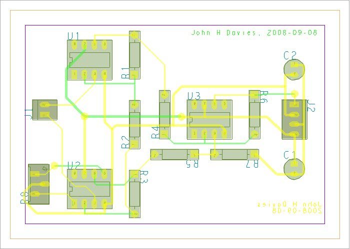
Figure 22. Double-sided layout after improving the layout and moving the badly-placed vias.
design may have none at all, which is a bonus. Remember to gloss or space and mitre the tracks.
5. Import the tracks into PCB Editor if you used PCB Router. Save the routed board under a new name.
You must move any vias in inconvenient places, such as that under U3 in figure 20. If you are lucky you may be able to Slide the via but it is often better to rip up the complete track and re-route it by hand. Other tracks must often be moved to create space for the via.
• Select the cline or net with the offending via, right-click and choose Delete or Ripup etch from the contextual menu.
• Select the connect tool and check in the Options control panel that the active and alternate layers are correct.
• Draw out the segments of the track as usual.
• Double-click when you reach the point where a via is needed. A via is inserted and routing switches to the alternate layer.
• Continue routing to complete the track.
I made several changes to the board to get the final version in figure 22.
• The via was moved from under U3 to a clear region of PCB.
• Another via was moved away from R8.
• The via near C1 was eliminated by rerouting the tracks slightly.
• Several tracks were moved from the top to the bottom, which makes the board easier to solder by hand.
• It would have been better to edit the board further so that all tracks leave the ICs on the bottom of the board. This would require extensive rerouting and more vias to be inserted. (Better still, I could have added a route keepout on the top layer of the footprint for the ICs. We have a local library with features such as this to help inexperienced students.) I also prefer to avoid vias in the tracks for power and ground.
When you have finished editing your board, add text to both layers of etch to identify them. It would be embarrassing if the top of your board was processed with the bottom of somebody else’s. Finally, plot the finished board in colour.
6 Artwork and drill files
The next step is to get the board made! Many routes are possible, depending on whether the board will be produced manually or automatically. You typically send a set of electronic files to a commercial manufacturer. Each company specifies its preferred formats and you should obviously follow this advice. Two types of file are typically needed.
• Artwork files contain images of the conducting (etch) layers and silkscreen, one file per layer. These are often known as gerbers after a well-known company, whose formats are widely used.
• Drill files provide a list of holes to be drilled, as you might guess, with their positions and diameter. These are often called excellon files after another company.
Further information, such as placement files, may be needed if the board is to be assembled automatically. Other processes may use ODB++ rather than artwork and drill files but lie far beyond the scope of this tutorial.
I’ll first explain how to produce photomasks directly from PCB Editor, which is useful if the PCB is made manually. The remaining sections show how to generate files for a commercial process.
6.1 Photomasks for manual production
This section shows how to get a black-and-white plot that can be printed onto tracing film to act as a photomask, which is used to manufacture your board manually. I’ll explain the most basic procedure here, which gives solid pads on the plot. Such boards may be drilled by hand as well, in which case it is helpful to leave open holes in the pads to guide the drill. Save your design before starting this procedure in case you make a mistake and wreck the board. The major step is to change the colours so that only the desired features are visible and to plot these in black.
Tip for Layout users: You will be used to similar manipulations with the post-processing and colour spreadsheets.

Figure 23. Part of the Color Dialog box, showing the settings for the Stack-Up to plot the bottom layer. Ignore the Pastemask_Bottom.
1. Open the Color Dialog box with Display > Color/Visibility. . . from the menu bar.
2. Click the button to turn Global Visibility Off, agree to Make all classes invisible in the small dialogue and click Apply in the main dialogue (this is needed after every change to see the effect). The design vanishes from the design window.
3. Click the Display folder in the list on the left. We must change the Background colour of the window so that tracks show up after their colour has been changed to black. Click on the white swatch in the Color swatches (samples of each colour) near the bottom of the window, then click the swatch next to Background, which turns white. Click Apply to update the design window, which also turns white.
4. Now we need make the desired features visible again and paint them black. Start by selecting Board Geometry from the list on the left. This brings up a set of Subclasses to the right. Select the checkbox next to Outline to turn it on. Change its colour to black by clicking in the black swatch in the Color region, then the swatch next to Outline. Finally, click Apply and the board outline becomes visible in the design window.
5. This must be repeated for all the features that we wish to print. For the bottom of a PCB these are Stack-Up/Conductor/Bottom/Pin, Via and Etch. Activate and make them black as shown in figure 23. Click Apply and your tracks appear, which completes the bottom of the PCB. Close the Color Dialog.
6. Check the Plot Setup. Set the Scaling factor to 1.00 so that the mask has the correct dimensions for the finished PCB. Leave the Default line weight as 10 or text may be too thin for reliable etching.
7. Finally, choose File > Plot. . . as usual and you should get a beautiful picture with the board outline and etch.
8. Repeat these steps for the top of a double-sided board. Deactivate the bottom subclasses and make the top ones active instead. Open Plot Setup and choose Mirror under Plot orientation.
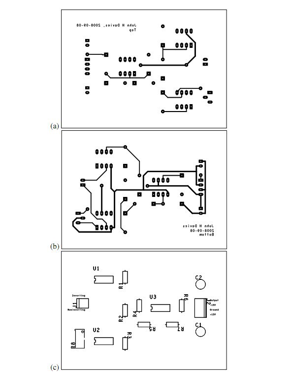
Figure 24. Printouts at actual size for the (a) top and (b) bottom of a double-sided board with (c) a silkscreen plot to assist assembly. Note that text appears mirrored on both the top and bottom. The plot must be mirrored because the printed side of the mask is turned over and placed next to the copper when the photoresist is exposed. A good check is that text should be mirrored on both masks for a double-sided board. (The text on the bottom is also mirrored on your computer’s screen but the text on the top is mirrored only on the plot.)
9. You might also wish to print a sort of ‘silkscreen’ to help you assembly the board. Use the same procedure and select the following classes.
• Package Geometry: Assembly_Top and Silkscreen_Top subclasses
• Components: All Cmp Val and Ref Des
Check the display: you may need to adjust this selection, depending on how your symbols were drawn.
Figure 24 shows my plots for the double-sided board. After all this, quit from PCB Editor without saving (or reload your design) to avoid messing up the colours next time you use it.
6.2 Drill files
This is the easy one! Choose Manufacture > NC > NC Drill from the menu bar and click the Drill button. PCB Editor writes a file with extension .drl in the widely accepted Excellon format. It is plain text so you can check it with a simple editor.
Open NC Parameters before creating the file if you need to change any settings to suit your manufacturer. European manufacturers may ask for metric drills, for instance. Choose Drill Legend from the menu if you want a drill chart. Each hole on the PCB is labelled with a symbol (hexagon, oval, . . . ), which is identified in a table that is added to the drawing. Layout users will find this familiar.
6.3 Artwork files for conducting layers
The next step is to produce an artwork file, also known traditionally as a film, for each con- ducting (etch) layer. The New Board Wizard had an option to Generate default artwork films which should have created settings for the top and bottom layers of etch. To preview these films, open the Visibility control panel and look in the drop-down list of Views. You should find Film: TOP and Film: BOTTOM. Select these to show the objects that will be drawn on the respective films: tracks, pads, vias and any other items that you added to the layers of etch.
Curiously there seems to be no way of restoring the original view other than reloading the design. Alternatively, open the Color Dialog (Display > Color/Visibility. . . from the menu bar or Color192 command), turn Global visibility On and turn off any unwanted classes.
Create the films
Define a photoplot outline before creating the films. This should be a rectangle that extends beyond the PCB. Choose Setup > Areas > Photoplot Outline from the menu bar (keepin photo command).

Figure 25. Film Control tab of the Artwork Control Form.
Click first to create one corner, then click again in the opposite corner to define the rectangle. Right-click and choose Done.
To create the films, select Manufacture > Artwork. . . from the menu bar (film param command), which opens the Artwork Control Form. Make the General Parameters tab active and choose the Device type that your manufacturer advises. The extended Gerber format with embedded apertures (RS274X) is widely accepted (the older RS274D format requires a separate list of apertures). You may receive a warning about the artwork accuracy. If this happens, increase the number of Decimal places in the Format section until the error goes away. The remaining parameters are probably satisfactory.
Return to the Film Control tab. It should resemble figure 25 except that the list of Available films contains only TOP and BOTTOM. Expand the tree for a folder to show the classes in- cluded in the film: etch, pin and via class. There is probably no need to adjust the Film options on the right for the etch layers unless you have included text, in which case you should enter a nonzero value for the Undefined line width. (The lines used to draw text have undefined width. Some manufacturers ask for text on etch layers to confirm which is top and bottom; the bottom should have mirrored text.)
Click the Select All button below the list, then on Create Artwork. A progress box ap- pears and, with luck, it concludes with Successfully Completed. Unfortunately it is often over- optimistic so you should click the Viewlog. . . button and check for warnings. Look out for undefined line widths in particular. The artwork files are called TOP.ART and BOTTOM.ART. They are plain text and can be opened with an editor if you are interested. Some manufacturers ask you to rename them so that their extension identifies the layer.
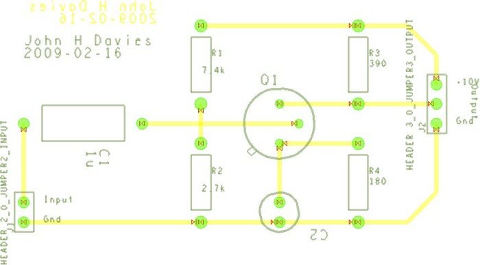
Figure 26. Review of artwork for top, bottom and top silkscreen films. The board outline is not included in the films.
Review the films
Review the artwork before sending it away. This is clumsy. Create a new board file and choose File > Import > Artwork. . . from the menu bar (load photoplot command, also called load gerber). Browse for one of the films that you have just created, TOP say. The dialog box should change to show the correct Format, such as Gerber RS274X. Leave the Origin at its default of Absolute Origin. Select the appropriate class and subclass, Etch/Top in this case, then click on Load file (not OK, which closes the dialog box, really irritating). A rectangle appears, centred on the cursor, so that you can place the imported image. Click on the P (Pick) button in the status bar below the windows, type coordinates of 0 0 into the Pick box and click Pick. This ensures that the image is precisely positioned so that all layers are correctly aligned. (If you have a steady hand you can instead move the mouse to coordinates of 0 0 as shown in the status bar and click in the design window.) Repeat for the bottom film; the Pick box remains visible and holds its previous entry so you just have to click on Pick. Click OK when you have imported all the films. Figure 26 shows the result except that I have included a silkscreen film as well, as I’ll explain in the next section.
Use the Visibility control panel to hide the layers of etch so that you can inspect each individually. I am not sure why the drawing is cluttered with DRC errors.
6.4 Silkscreens
Many classes of the database contain information in a silkscreen subclass so these must first be merged to produce a complete silkscreen. Choose Manufacture > Silkscreen. . . from the menu bar to open the Auto Silkscreen dialog box (silkscreen param command). Most of the options are reasonably clear. You may wish to turn off unwanted classes and subclasses, such
as Tolerance and User part number, by selecting None. Click the Silkscreen button when you have finished. PCB Editor then merges the separate silkscreen subclasses into the Autosilk_Top and Autosilk_Bottom subclasses of the Manufacturing class and displays the result. Check the command window for any errors.
The design looks cluttered if both the individual silkscreens and the new, composite silk- screens are displayed. Hide the individual silkscreens by opening the Color Dialog, selecting the components folder, and turning all items off with the top left check box. (Alternatively, use the button next to each class in the Options control panel.) You may also wish to deselect further silkscreen subclasses of Board Geometry and Package Geometry.
The next issue is how to write a file or files with the silkscreen data (I’ll assume that there is only a top silkscreen). It can be printed but the most common route is to create an artwork file like those for the etch layers. No films for silkscreens are defined by default so here is the procedure for creating them.
1. Open the Color Dialog, turn Global visibility off, then go to the Manufacturing folder and turn Autosilk_Top back on. Click OK, which leaves only the (top) silkscreen visible in the drawing.
2. Open the Artwork Control Form with Manufacture > Artwork. . . . Right-click on one of the available films and choose Add. (Do not try the Add. . . button, which is for selecting a previously created film record.) Give the new film a name such as Silkscreen_Top. It includes the classes that are currently visible in the drawing and is added to the list of available films.
3. Select the folder for the newly added film in the list, which brings up its options in the right-hand panel. Enter a nonzero value for the Undefined line width. A suitable value is
10 (mils); a smaller value is unacceptable to some manufacturers because silkscreens are produced at lower resolution than etch. This step is essential because many lines in the silkscreen have undefined width and are useless if they are drawn with a width of zero.
4. Select the checkbox for the new film and click Create Artwork. The photoplot log file will almost certainly appear with plenty of warnings. These are no problem if they warn you that the undefined line width has been used for 0 width lines and text. Otherwise, check.
5. Review the .art file as usual.
Further films are needed for the soldermask(s) and some manufacturers ask for a film with the board outline alone. Make these in the same way.