A basic introduction to
Cadence OrCAD PCB Designer
Version 16.3
Professor John H. Davies
Department of Electronics and Electrical Engineering Glasgow University, Glasgow, G12 8QQ, Scotland, UK Email: jdavies@elec.gla.ac.uk
2011 October 6
Contents
Preamble
1 Introduction
2 One-transistor amplifier: Schematic capture
3 OrCAD PCB Editor
Preamble
This document introduces the basic features of OrCAD PCB Designer. It is aimed primarily at novices with limited experience of construction who have never designed a PCB before. For this reason I concentrate on pin-through-hole devices (although surface-mount devices are no more difficult) on single and double-sided boards. I strongly recommend Mitzner’s book [1] instead if you are an experienced designer, interested in more advanced PCBs for commercial production.
Other readers may be experienced users of OrCAD Layout who are obliged to switch to PCB Editor; I hope that they don’t feel that their intelligence is insulted! I’ve highlighted some of the most significant differences between Layout and PCB Editor. (I think that PCB Designer refers to the complete suite while PCB Editor is the specific application for editing PCBs but it’s not entirely clear.)
I adapted this document from an introductory class and have removed several features that are unlikely to be of interest to most readers. For example, we have developed a local library of footprints for PCBs constructed by students. The pads are enlarged to allow easy soldering and the symbols contain features to discourage common design errors, such as tracks to inaccessible pads underneath connectors. However, I’ve retained the instructions to produce photomasks directly with the Plot command, rather than with Gerber files. This is helpful if you make PCBs in-house by traditional processes, which is often the case for student projects.
Differences between versions 16.0, 16.2 and 16.3
Version 16.3 of OrCAD was released in late 2009, following 16.2 in late 2008. The What’s New document exceeds 90 pages but most of the changes aren’t relevant to an introductory tutorial. Here are the most important new features in version 16.2.
• The appearance of Capture has been updated to match PCB Editor. Buttons are now larger and their purpose is sometimes clearer. A bar of tabs can be used to switch between windows.
• Cross-probing between Capture and PCB Editor has been improved.
• The Plot command can leave drill holes open, which may be helpful for PCBs drilled by hand.
• The software is installed in the same way, regardless of whether you have a licence or not.
Applications simply run in demonstration mode if they cannot find a licence. The demo version is a great improvement on previous editions but the installer has a peculiarity: you are forced to specify a licence server even if you wish to use only the demo mode. A bogus server such as 5280@localhost should get around this problem.
This tutorial is affected less by changes from 16.2 to 16.3.
• A board can now be ‘flipped’ (viewed from underneath rather than from the top) and rotated in 3D but this is of limited value for the simple designs described here.
• Jumpers have been added to assist the design of single-sided boards.
• The autorouter is now called Allegro (or OrCAD) PCB Router rather than SPECCTRA.
Board files written by version 16.3 of PCB Editor cannot be read by version 16.2, nor can those written by 16.2 be read by version 16.0. (This contradicts the statement in Getting Started with Physical Design that ‘Allegro PCB Editor databases are backward-compatible with their major version number (the number to the left of the dot)’.) Use the menu item File > Export > Save design to 16.2. . . (or 16.01. . . ) to write a file compatible with an earlier version. (The jargon is to downrev the design.) I have not yet updated this document for version 16.5.
1 Introduction
The Cadence OrCAD PCB Designer suite comprises three main applications.
• Capture is used to draw the circuit on the screen (schematic capture). A netlist, which describes the components and their interconnections, is the link to PSpice and PCB Edi- tor.
• PSpice simulates a captured circuit. I do not describe PSpice in this tutorial.
• PCB Editor (Allegro) is the application for laying out a printed circuit board. It includes an automatic router that works out the arrangement of tracks needed to connect the com- ponents on the PCB. The output from PCB Editor is a plot or a set of files that can be sent to a manufacturer.
The overall design flow for making a PCB is shown in figure 1.
PCB Editor replaces the earlier application, Layout, which is now discontinued. OrCAD PCB Designer is the most basic version of Cadence’s Allegro suite for PCB design and much of the documentation refers to ‘Allegro’ rather than ‘PCB Editor’.
Fixup. The libraries for Capture and PCB Editor have some incompatibilities that must be corrected by Fixups. I hope to find smoother ways around these difficulties in the future.
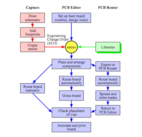
Figure 1. Design flow for making a PCB with Capture and PCB Editor. The three paths for PCB Editor depend on whether the tracks are drawn manually (as in the first design), automat- ically within PCB Editor, or by running the autorouter as a separate application.
1.1 Libraries, files, directories and design rules
Three types of information are needed for each component, corresponding to the three main applications listed above.
• Electrical symbols are used to draw the circuit in Capture.
• Electrical models allow you to simulate the circuit in PSpice.
• Footprints or package symbols show the physical size and shapes of the pads (where the pins are soldered to the board) and the outline of the package. They are used to lay out the circuit in PCB Editor.
These are stored in different sets of libraries and you must select the files needed for a particular design. Footprints are needed as well as electrical symbols because components with the same electrical behaviour come in different packages. For example, an integrated circuit might come in two versions:
• a traditional, plastic dual-in-line package (PDIP) with pins 0.100 apart
• a smaller, surface-mount device (SMD) with pins only 0.5 mm apart, if it has pins at all
The opposite is also true: resistors of a particular shape come in a wide range of values.
Further information is needed to describe the characteristics of the printed circuit board on which the components are mounted. The details are important for high-speed designs but we need to know only the number of layers of copper, called etch in PCB Designer. This tutorial covers only single-sided boards, which have components on top and copper on the bottom, and double-sided boards, which have copper on both surfaces but usually components only on the top. Fancier boards often have two internal planes of copper used for power and ground; complex designs need further layers.
Design rules are required to lay out the circuit on the PCB. The full details are complex but the basic rules specify the minimum width of tracks and the gap between them. Manufacturers often express these numbers in the format 10/8, meaning minimum widths of 10 for tracks and
8 for gaps (although the numbers are usually the same). The units are almost always mils, which mean thousands of an inch; see section 2.5 on page 10. I use 25/25 rules in this tutorial, which are extremely coarse but produce boards that are easy for inexperienced students to solder.
Further design rules control a diverse range of features, such as the spacing between tracks and pads, whether vias are permitted and the impedance of tracks (they act like transmission lines at high frequency). These rules are adjusted with the Constraint Manager, which we’ll encounter in section 4.4 on page 29.
Fixup. Older versions of OrCAD prefer designs to be stored in OrCAD_Data rather than My Documents and may reject filenames that contain spaces. If you get inexplicable errors about unexpected arguments or incomplete file names, try copying the design to OrCAD_Data and
removing spaces from the names of all directories and files.
1.2 Help!
All programs provide extensive online help. Many commands in PCB Editor have names that are not obviously related to the corresponding item on the menus so I have pointed these out.
2 One-transistor amplifier: Schematic capture
The first design is a one-transistor amplifier. It has only a few components and will be laid out on a huge board to make the routing straightforward: The challenge is to learn the software. The initial step is to draw the circuit in Capture.
Capture treats each circuit design as a project and a project manager shows the logical relation between the files required. It is essential to create a new directory for each project. Strange errors can occur if you have more than one project in a directory, from which it seems impossible to recover. It also keeps your work organised. OrCAD creates a subdirectory for PSpice files and an allegro subdirectory for PCB files. You should know this by now but a reminder is never a bad idea: Save your work frequently and take regular backups of important circuits.
Note. I have wasted hours trying to reconstruct projects where students have not obeyed the rule of one project per directory! I don’t know why they find it so difficult.
Select Start > Programs > OrCAD 16.2 > OrCAD Capture. I use ‘>’ throughout this document to show the levels of a hierarchical menu. There will be a short delay while the software is loaded and the licence server is accessed. Alternatively, you will be asked if you wish to use Demo mode if no licence can be found. The screen then shows the OrCAD Capture main window with a menu bar and various toolbars. A sub-window at the bottom shows the session log; its title may be hard to find if the window has been docked. Version 16.3 offers different ways of controlling the windows; right-click in a title bar.
2.1 Create a project
The first step in OrCAD is always to create a project.
1. Create a new directory in Windows to hold all files for the project.
2. Select File > New > Project from the menu bar of Capture.
3. In the New Project dialog box:
• Select an Analog or Mixed A/D project if you wish to simulate the circuit. You could use the PC Board Wizard or Schematic options if you don’t want to simulate the circuit, in which case the steps differ slightly from my description.
• Click on the Browse key and navigate to the new directory that you created for this design. Click OK.
• Give the project a meaningful name.
• The path and directory now show in the location box (if you can see them – they are usually too long). Click OK in the New Project dialog box.
• Click Next.
4. Select the Create a blank project button in the small dialog box that appears and click
OK.
5. Your project will now be created. The Project Manager window at the top left shows the files associated with your design and the resources used, such as library files. Its title is the full pathname of your project, which is usually far too long to fit. Make the File tab active if necessary.
6. Expand the Design Resources folder in the project, then the design (called ./project- name.dsn, where project-name is the name of your project), then the SCHEMATIC1 folder and finally double-click PAGE1 to open the schematic page for your design. Lo- cate the Title box in the lower right-hand corner, double-click on the placeholders, which are in angle brackets <>, and replace them with a descriptive title and so on.
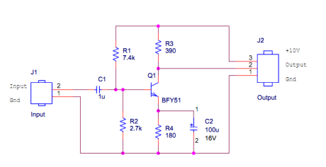
Figure 2. Schematic drawing of a simple, one-transistor amplifier. The pin numbers on the electrolytic capacitor are not normally visible but are shown to illustrate a fixup later.
2.2 Draw the circuit
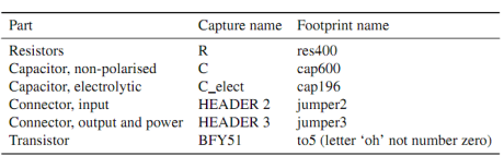
Draw the circuit shown in figure 2. The names of the components are listed in table 1; I’ve renamed some of them to make their functions clearer. I assume that you are familiar with Capture but here are a few tips to help.
Jargon: The label that identifies each component on the schematic drawing is called its refer- ence or refdes, short for reference designator. For example, the transistor has refdes Q1. Each
refdes must be unique: No other component can be called Q1.
• I used libraries from the pspice folder so that the circuit could be simulated although I do not describe that here. Basic components like resistors are in the analog library. The connectors are in the connector library, which is in the directory one level above the pspice directory (OrCAD16.3/tools/capture/library/). Use Search if you can’t guess where a component is located. You may need to do this for the transistor.
If you have no intention of simulating the circuit you might prefer to use components from the discrete library instead of pspice/analog. This avoids a problem with the num- bering of pins that will arise shortly.
• The capacitor C2 is an electrolytic type, which must be installed with the correct polarity or it will explode. One of its plates on the schematic is therefore labelled with a + sign and must be connected to a positive voltage. (Its pin numbers are also shown because of a fixup later.) The parameter CMAX is the maximum working voltage of the capacitor, which is not needed for simulation but important when you pick out the real component. I set it to 16 V, which is a common value.
• Always join components with wires, not by placing them so close that their pins overlap.
This can cause strange errors.
Table 1. Components, names in Capture and footprints for the one-transistor amplifier. These are taken from the library supplied with PCB Designer. The names are not case-sensitive.
• Wires and components sometimes become joined incorrectly if you move them about.
Use Place > Junction or the junction tool from the toolbar on the right to eliminate spurious connections.
• Include connectors for all wires that leave the PCB. This includes inputs, outputs and the power supplies. It is a good idea to change the ‘values’ of connectors to make them more descriptive than the defaults, for example Input rather than HEADER 2. Do not edit the reference, such as J1.
• Add text to label the pins of each connector.
Print the drawing sheet: You will need this soon to guide the layout of your PCB. This circuit takes up only a small part of the page so it is a good idea to choose File > Print Area > Set and mark out a rectangle that includes only the part of the page that you wish to print. Check the circuit carefully – it is much easier to correct mistakes at this stage.
Note. The Place Part dialog box is a pop-out panel in version 16.3 and its appearance has been modified considerably from the traditional version. The functionality is unchanged. Click on the ‘pin’ icon in the title bar to fix it if you prefer.
Some students change the Reference (J1 or J2) of the connectors to Input or Output instead of changing the Value (HEADER 2 or HEADER 3). This upsets the netlister later.
2.3 Preparation for PCB layout
The procedure to this point should be familiar if you have used Capture with PSpice. A few extra steps are needed to prepare the schematic for a PCB.
Fixup. The electrolytic capacitor C_elect in the pspice/analog library is incompatible with its footprint. The pins of the footprint are numbered 1, 2 but those of the capacitor are p, n. This means that the software cannot match the capacitor to its footprint. Edit the electrolytic capacitor and change the numbers of its pins to resolve this.
1. Select the electrolytic capacitor and choose Edit > Part from the menu bar. A window opens with an enlarged view of the capacitor.
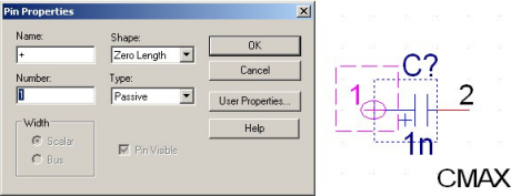
Figure 3. Edit Part window and Pin Properties dialogue box for correcting the numbering of the pins of the electrolytic capacitor.
2. The positive pin is shown as a circle on the left. Select it and and choose Edit > Proper- ties. . . . This brings up the Pin Properties dialogue box, shown in figure 3.
3. Change the Number to 1 and click OK. Don’t worry about the name of the pin.
4. The negative pin is shown as a red line on the right. Change its Number to 2.
5. Choose File > Close. You have the choice of updating this part alone, or all ‘part in- stances’ – that means all C_elect components in your design. There is only one so it doesn’t matter whether you choose Update Current or Update All in this case.
I made the pin numbers visible for the electrolytic capacitor in figure 2 as a reminder of this fixup. You need not do this.
This problem can be avoided by using components from the discrete library instead, which is in the directory one level above the pspice directory. However, these components are not associated with pspice models and therefore cannot be used for simulation.
The main task in preparing the design for layout is to associate a footprint with each com- ponent. The footprint shows the physical outline of the components including the copper pads to which the pins are soldered. Most pads are either circular or oval except for pin 1, which has square corners to identify it. The components in many Capture libraries have footprints already but unfortunately they are mostly wrong. We must therefore enter the correct footprints, which are listed in table 1 for this circuit. Don’t muddle the letter ‘o’ with the numeral ‘0’. The whole business of assigning footprints is unnecessary if you have a database of components in Capture CIS.
1. Drag the cursor over your schematic drawing so that all the components are enclosed in a rectangle. Do not include the title box.
2. Choose Edit > Properties. . . from the menu bar, which brings up the Properties spread- sheet.
3. Type each name into the PCB Footprint field of the Properties spreadsheet. All the resistors have same footprint so use copy and paste for speed.
Tip for Layout users: PCB Designer comes with a small library of footprints compared with the extensive libraries that were provided with Layout. I’ve been told that this is because most users have their own libraries. Where there is a need, somebody will offer a service: Online libraries of footprints are available – for a fee.
PCB Editor has no convenient way of copying the names of footprints into Capture from a library, as in Layout.. PCB Editor also
lacks anything like the library manager in Layout.
2.4 Design rules check
The next step is a Design Rules Check to ensure that no errors have been introduced.
1. Click on the Project Manager window and highlight your design (with extension .dsn).
2. Select Tools > Design Rules Check. . . from the menu bar.
3. Under Design Rules select both Run Electrical Rules (probably selected already) and
Run Physical Rules (probably not).
4. Click OK. A dialog box may report One or more errors or warnings were encountered.
Do you wish to view the messages in the session log? Agree to this and review the report in the Session log window. No positive message is given to confirm that all rules have been passed successfully, just an absence of complaints. Ask for help if you do not understand a message – don’t just ignore it.
5. Return to your drawing and correct any errors, shown by green circles (a strange choice of colour). Repeat until the Design Rules Check runs silently.
6. You may wish to run the Design Rules Check and select Action > Delete existing DRC
markers to get rid of the green circles. They do not vanish by themselves.
2.5 Make a bare board in PCB Editor
The simplest way of creating a PCB is first to set up an empty PCB, then to add your compo- nents and connections to the board. This follows the design flow shown in figure.
First create a directory allegro within your directory for the current project. PCB Editor likes to keep its files here. Choose Start > Programs > OrCAD 16.3 > OrCAD PCB Editor, which opens the OrCAD PCB Designer application (Cadence seem muddled about the name). I’ll leave the details of the interface until later because we need only one dialogue box for this step.
Choose File > New. . . from the menu. In the first dialogue box, set the Drawing Type to Board (wizard). Click Browse. . . , navigate to your new allegro directory and give the board a name such as bare.brd. Click Open then OK to bring up the new board wizard. This takes you
through several screens to define the parameters of the PCB. Some of these are obvious, such as the size of the board, while others set up the design rules – the width of tracks on the PCB, how much space must be left between them, and so on.
1. The first screen is purely descriptive. Read it, then click Next >.
2. This asks for a board template. We don’t have one so select No (probably the default)
and click Next >.
3. You are next asked for a ‘tech’ file. This is short for a technology file, which specifies the design rules. Again we don’t have one so select No and click Next >.
4. This asks for a board symbol. Select No again and click Next >.
5. We now reach the screens for the parameters that must be set up. The units should be Mils. These are not millimeters but the American term for thousandths of an inch;
1 mm ? 40 mils. All dimensions are given in these units so get used to them.
Leave the drawing size at A. This is an American size but you aren’t allowed European
A4 if the units are mils. Leave the origin at the centre.
6. Set the grid spacing to be 100 mils.
The Etch layer count is the number of copper layers on the board – the number of layers of tracks for signals and power. Leave this at 2, although we shall use only one layer in the first design.
Select Generate default artwork films, which is the default.
7. Leave the names of the layers as Top and Bottom and their types as Routing Layer.
8. Enter 25 for the Minimum Line width (in mils). This value propagates into the other boxes. It means 0.02500 or about 0.64 mm, which is very wide for a track nowadays but makes the board easy to solder by hand.
For the Default via padstack, click on the button with . . . and choose Via26. This design is far too simple to need vias, which carry a signal from one layer of the PCB to another, but they may be required later.
9. Rectangular board (it’s curious that a circular board is the default).
10. Enter a width of 3000 and height of 2000 mils. This defines the board outline as 300 × 200.
There is no corner cutoff.
Specify the Route keepin distance as 100. A keepin means that objects must be kept inside the specified region. In this case it means that tracks cannot go any closer than
100 mils to the edge of the board. It gives a border around the PCB to aid handling and manufacture. (We’ll encounter keepouts as well later.)
Set the Package keepin distance to 250. Components must be placed within this keepin and therefore cannot be closer than 250 mils to the edge of the board. The gap between the two keepins allows you to run tracks around the outside of all the components, which is often helpful on a more complicated board (although hardly necessary here).
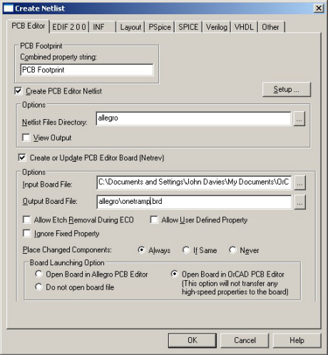
Figure 4. Completed dialogue box for netlisting the design and sending it to PCB Editor. Your file names will be different.
11. Click Finish – that’s it.
This has set up the design rules and made an empty board, which you can see in the design window of PCB Editor, shown in figure 5. Three rectangles are visible for the board outline, route keepin and package keepin. Choose File > Save and close PCB Editor.
The next step is to return to Capture and send the circuit to PCB Editor so that it can be added to the bare board.
Tip for Layout users: PCB Designer does not come with a library of technology files, as did
Layout. Cadence expect you to have your own. Fortunately it is easy to export a tech file from a board file that you have set up to your liking;
2.6 Create a netlist
The information about your design is sent from Capture to PCB Editor in the form of a netlist, which contains a description of the circuit and its components. (The netlist comprises three files but you rarely need to look at them.)
1. Highlight your design (the object whose name ends in .dsn) in the Project Manager window of Capture.
2. Select Tools > Create Netlist. . . from the menu bar, which brings up the dialogue box in figure 4. Make sure that the PCB Editor tab is active.
3. Confirm that the PCB Footprint box contains PCB Footprint and that the box underneath for Create PCB Editor Netlist is selected.
4. Under Options, the Netlist Files Directory should be shown as allegro. Select Create or Update PCB Editor Board (Netrev). Netrev is the application that merges the netlist, footprints and other information into the database used by PCB Editor, hence its central position in figure 1.
5. For Input Board File, choose the bare board that you have just set up. Click on the ‘. . . ’
button to navigate.
6. The Output Board File usually shows something sensible automatically; edit it if not. It should use the new allegro directory.
7. Under Board Launching Option, select Open Board in OrCAD PCB Editor if your li- cence doesn’t cover the full version of Allegro.
8. The entries in the dialogue box should now resemble figure 4 except for the pathnames. Click OK to dismiss this dialog box and start the netlister.
You are warned that your design will be saved by Capture, then a Progress box shows the various processes needed: Netlisting the design followed by Updating OrCAD PCB Editor Board. PCB Editor is then launched with your new board.
• You may see a Warning box, which tells you that Netrev succeeded with warnings.
Check the Session Log if this happens. Messages about RVMAX and CMAX can be ignored; these are maximum voltage ratings of the components and are not important for this circuit. Pay attention to any others!
• OrCAD PCB Editor gives you a warning that Database was last saved by a higher tier tool, which you can ignore.
You should now see your empty board outline on the screen of PCB Editor again; the compo- nents have been added to the database but are not yet visible.
Note. The netlister in some versions of 16.x has a nasty bug (the pxllite bug). The symptoms are that the Netlist Files Directory does not show as allegro automatically in figure 4 and that nothing happens when you run the netlister – not even an error mes- sage. Netlisting for PCB Editor must be performed once on each computer by a user with administrator privileges before it will work for anybody else.
PCB Editor is almost always launched even if there was a fatal error during netlisting: It is vital to check the session log. Many students don’t bother, and discover only later that components are missing.
Check the search paths if PCB Editor complains that it can’t find components. This shouldn’t occur if you use the standard libraries but may arise with local libraries. Choose Setup > User Preferences. . . from the menu bar, which brings up the User Preferences Editor, then look at
Design_paths in the list of Categories. ?
Tip for Layout users: This process is similar to creating a netlist in Layout – it just uses a different tab in the Create Netlist dialogue box.
Where are my components? Layout automatically displays the components on screen, ready for you to move on the PCB. Allegro does not do this: You must place them yourself. The Quickplace command achieves the same effect
as Layout.